Shift Register Rtl Diagram : PPT - Shift Registers and Shift Register Counters ... / Srclk (shift register clock) is the clock for the shift register.
Get link
Facebook
X
Pinterest
Email
Other Apps
Shift Register Rtl Diagram : PPT - Shift Registers and Shift Register Counters ... / Srclk (shift register clock) is the clock for the shift register.. Gnd should be connected to the ground of arduino. The logic diagram of a 4 bit universal shift register is shown below. This sequential device loads the data present on its inputs and then moves or shifts it to its output once every clock cycle, hence the name shift register. Register to load and store binary value. Vcc is the power supply for 74hc595 shift register which we connect the 5v pin on the arduino.
It has a wide operating voltage from 2v to 6v. A shift register of generic length. Gnd should be connected to the ground of arduino. In that case input is feed from right side and output is getting from left side. This sequential device loads the data present on its inputs and then moves or shifts it to its output once every clock cycle, hence the name shift register.
alex9ufo 聰明人求知心切: The SISO SIPO PISO PIPO Shift Register ... from 2.bp.blogspot.com Similarly, the value of the mode is chosen as 0 the circuit operates as left shift register. The mode input is connected to high (mode = 1); The logic diagram of a 4 bit universal shift register is shown below. This means that in order to shift bits into the shift. 7.0 shift register counters two of the most common types of shift register counters are introduced And for serial shifting, the mode input is connected to low (mode = 0). This sequential device loads the data present on its inputs and then moves or shifts it to its output once every clock cycle, hence the name shift register. I'm not necessarily asking for a schematic diagram so much as i'm looking for an explanation of how such a circuit might be built.
The registerladder logic diagrams are targeted for implementation in field programmable gate arrays.
The timing diagram for the system is as shown in the image below; Because all flops work on the same clock, the bit array stored in the shift register will shift by one position. 7.0 shift register counters two of the most common types of shift register counters are introduced Bidirectional shift registers are the storage devices capable of shifting the data either right or left, depending on the mode selected. The following image shows an. Srclk (shift register clock) is the clock for the shift register. It has a wide operating voltage from 2v to 6v. A shift register of generic length. Coding guideline, rtl examples and basics. The registers are capable of loading and retrieving the data. Here is a sipo, the 74hc595, and the piso, the 74hc165. An application circuit of the ic is shown below: Microoperations category arithmetic, logical and shift.
This means that in order to shift bits into the shift. It is different in that it makes all the internal stages available as outputs. At interval t 5 , the registered is configured to shift right and at t 8 towards Vcc is the power supply for 74hc595 shift register which we connect the 5v pin on the arduino. To load the data in parallel.
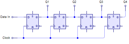
Introduction : SHIFT REGISTERS from www.learningelectronics.net Gnd should be connected to the ground of arduino. This is a special case of shift registers. This sequential device loads the data present on its inputs and then moves or shifts it to its output once every clock cycle, hence the name shift register. It is different in that it makes all the internal stages available as outputs. Sipo or piso shift registers. It requires only 3 pins connected to the mcu, which are clock, data and latch. Multiply, compare, bit shift, etc.) hlsm conventions hlsmswe discuss will follow these conventions: The functional diagram of the shift register is shown below;
Shift left register for shift left register the reverse action takes place.
At interval t 5 , the registered is configured to shift right and at t 8 towards Coding guideline, rtl examples and basics. All inputs, outputs and local storage are defined at the top of the hlsm diagram bit lengths are included in this definition registered outputs must be. It is different in that it makes all the internal stages available as outputs. The first type, sipo, is useful for controlling a large number of outputs, including leds, while the latter type, piso. Gnd should be connected to the ground of arduino. Multiply, compare, bit shift, etc.) hlsm conventions hlsmswe discuss will follow these conventions: The mode input is connected to high (mode = 1); Ser (serial input) pin is used to feed data into the shift register a bit at a time. The circuit diagram of a 4 bit bidirectional universal shift register is shown below. Shift register (sipo & pipo mode)contribute: I'm not necessarily asking for a schematic diagram so much as i'm looking for an explanation of how such a circuit might be built. What are universal shift registers?
In the rtl design methodology different types of registers such as counters, shift register, sipo (serial in parallel out), piso (parallel in serial out) are used as the basic building blocks for any sequential logic circuits. This means that in order to shift bits into the shift. It requires only 3 pins connected to the mcu, which are clock, data and latch. Register to load and store binary value. The registers are capable of loading and retrieving the data.
LEDs and Bit Shifting: A Shift Register tutorial from upload.wikimedia.org And for serial shifting, the mode input is connected to low (mode = 0). It requires only 3 pins connected to the mcu, which are clock, data and latch. The rtl verilog design of timing, counting, drum counter and shift register operations using ladder diagram for programmable controller. The timing diagram for the system is as shown in the image below; Microoperations category arithmetic, logical and shift. A shift register of generic length. In this article we try to explain the fundamental differences between register transfer level (rtl) design and sequential logic design. The functional diagram of the shift register is shown below;
7.0 shift register counters two of the most common types of shift register counters are introduced
Because all flops work on the same clock, the bit array stored in the shift register will shift by one position. To load the data in parallel. Multiply, compare, bit shift, etc.) hlsm conventions hlsmswe discuss will follow these conventions: The registers are capable of loading and retrieving the data. If the mode is set to high that is selected as 1 then the circuit operates as right shift register. The circuit diagram of a 4 bit bidirectional universal shift register is shown below. All inputs, outputs and local storage are defined at the top of the hlsm diagram bit lengths are included in this definition registered outputs must be. Similarly, the value of the mode is chosen as 0 the circuit operates as left shift register. And for serial shifting, the mode input is connected to low (mode = 0). This means that in order to shift bits into the shift. A shift register of generic length. See the block diagram of shift left register in bellow. At interval t 5 , the registered is configured to shift right and at t 8 towards
Srclk (shift register clock) is the clock for the shift register rtl diagram. Shift registers 1.0 introduction shift registers are a type of sequential logic circuit, mainly for storage of.


Comments
Post a Comment